If I made a Christmas wish-list, the SNES Classic would be on it.
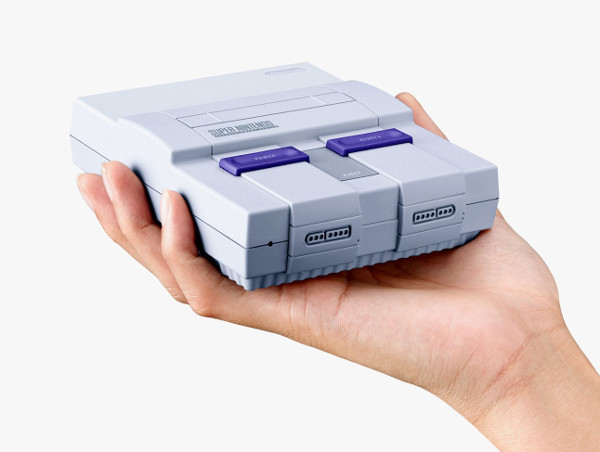
I finally found one on the store shelf. When I got it home I played me some Star Fox and Super Metroid, and then of course I took the poor thing apart.
The power adapter and cable are standard USB and Micro-USB, so it’s official as far as I’m concerned: USB is the standard for low voltage DC power, and it just happens to also include a data link.
Nintendo used to be a huge fan of security screws, but I didn’t run into any triwings or anything else goofy, here, just ordinary #0 Phillips.

That little wisp of a cable connecting the main board to the power switch and reset button confirms that the power switch does not switch the power. This device is always on, and it’s software that responds to the power switch state. The reset button isn’t a reset either, of course, it’s essentially a “home” button.
If the controller port cover thing annoys you, you can remove it. You might be able to detach it without even opening the system, and you can certainly reinstall it without taking out screws.
That’s a mean amount of shielding on that board, but that big piece of metal might be more important as a heat sink. We’ll definitely find an interesting chip under that depressed square area.
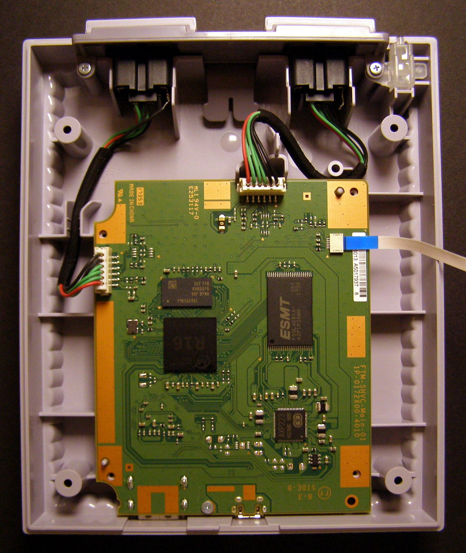
The interesting chip is an Allwinner Technology R16, an ARM Cortex-A7 with half a meg of L2, a (10-year-old!) GPU supporting OpenGL ES 2.0, and a 1080p video encoder. Apparently it’s marketed as an IoT component, so if you’re wondering how much processing power your WiFi toaster has, it may be enough to emulate an SNES.
The other, nearby BGA chip is 512MB of DDR3 RAM. Obviously this thing’s performance blows the face off an actual SNES. From a historical perspective, this cute little computer probably could’ve won the Nazis the war.
The large ESMT chip is a F59L4G81A, which is 512MB of Flash memory. That surprises me, actually, I expected more. Not that you need much more; compressed SNES games range in size from half a meg up to two megabytes or so. Still, you aren’t going to hack this thing to contain every single game ever released without adding storage.
The small chip to the lower-right with the posse of inductors and capacitors around it is an AXP223, a PMIC. Here it’s just doing power supply duty, generating different voltages and such, but it does have hilarious extra features including a camera flash charging circuit.
There’s one more chip hiding on the other side of the board:
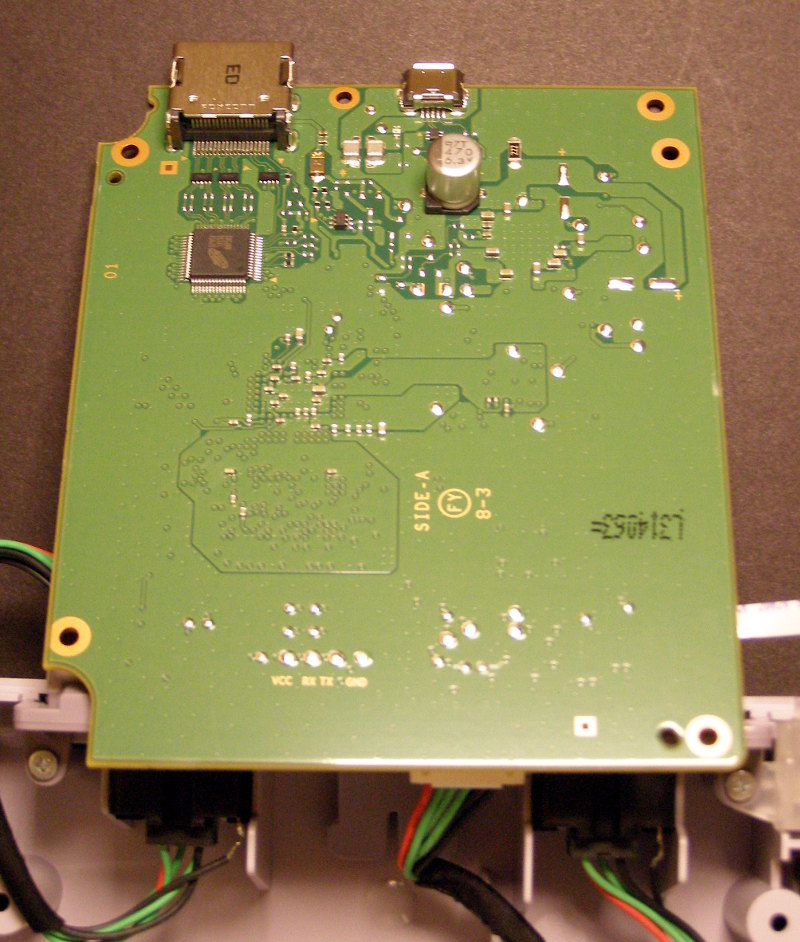
It’s an EP952 HDMI transmitter. Basically it combines audio and video data, does the whole HDCP thing, and generates the signals for the twisted pairs leading off to your TV.
If you look closely at the board, you’ll see that the Micro-USB port’s data lines are connected to the CPU. It’s not just for power, this is a USB device. This is what the Linux kernel said when I plugged it in:
   usb 2-1.3.4: new high-speed USB device number 118 using ehci-pci

   usb 2-1.3.4: New USB device found, idVendor=057e, idProduct=2044

   usb 2-1.3.4: New USB device strings: Mfr=1, Product=2, SerialNumber=3

   usb 2-1.3.4: Product: CLV-S-SNSY

   usb 2-1.3.4: Manufacturer: Nintendo Co., Ltd

   usb 2-1.3.4: SerialNumber: 873c9cd6d7676c118000
Overall this adorable miniature Super Nintendo is well-made, but its controllers maybe not so much. See the bottom of this post for the teardown of one of the controllers.


